Today in this tutorial i'll explain you how to control 74HC165 parallel in serial out(PISO) shift register using your ARDUINO board.Here we used 74HC165 for increasing numbers of inputs of your ARDUINO board.Shift registers are often used for the purpose of saving pins on a microcontroller. Every microcontroller has a limited number of pins for general inputs and outputs (GPIO).Some time we have required more inputs and our controller does not provide such a inputs at that time parallel in serial out(PISO) shift register is used to increase inputs.
An 8 bit shift register needs 4 lines of a microcontroller. One pin to clock for data transfer,one for clock enable,one for shifting/loading/latching the bits,and one for serial data transfer.Here we used only 3 pins of microcontroller. One pin for loading the bits,one pin to clock for data transfer,one pin to serial data transfer.In 74HC165 Clock enable pin is active low so we connect it to ground.Two 74HC165 can be cascaded to increase lots of inputs.
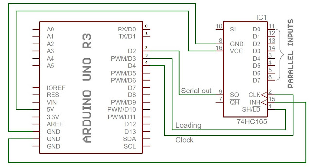
As shown in above connection diagram
 |
| Pin Diagram 74HC165 |
Show in above image the input pins of the shift register 74HC165 are pin 11 to 14 (D0-D3 Lower 4-bits) and pin 3 to 6 (D4-D7 Higher 4-bits).According to the datasheet of 74HC165 the maximum allowable voltage for VCC is 7V, where the input voltage range is between GND to VCC. But our arduino board having inbuilt 5V so it is recommended to operate the at 5V.
74HC165 has three control pins to control shift register and two output pins which are listed below
- CP - Clock Input (LOW-to-HIGH edge-triggered),
- /CE - Clock Enable input (active LOW)
- /PL - Asynchronous parallel load input (active LOW)
- DS - Serial data input , used when you want to cascade two or more shift register together.
- Q7 - Serial output from the last stage
- /Q7 - Complementary output of Q7 from the last stage
Working of 74HC165:
According to the datasheet you need to make the Parallel load input high.When the
parallel load (PL) input is trigger LOW, parallel data from the D0 to D7 inputs are loaded into the
register asynchronously.
When PL is HIGH, data enters the register serially at the DS input and shifts one place to the right (Q0 ---> Q1 ---> Q2, etc.) with each positive-going clock transition. This feature allows parallel-to-serial converter expansion by tying the Q7 output to the DS input of the succeeding stage.
Now, Send the clock pulse(LOW-to-HIGH) to the shift register to obtain the serial output. At that time you need to set /CE pin to low to enable clock input. 8-bit parallel data will be sent out in eight clock pulse.
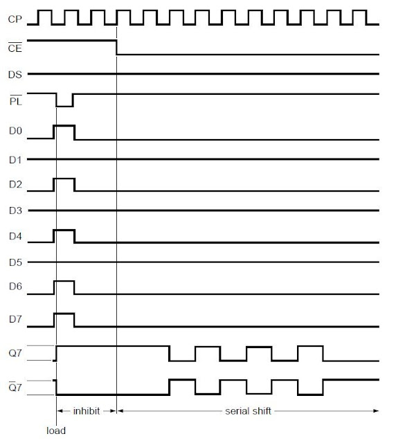
Show the shift register operation in Timing diagram
 |
Timing Diagram |
Connection With Arduino UNO:
 |
74HC165 with Arduino UNO |
- SO-Serial output (Pin 9) of 74165 is connected to the digital pin 2 of Arduino UNO.
- SH/LD (Pin 1) of 74165 is connected to the digital pin 3 of Arduino UNO.
- CLK (Pin 2) of 74165 is connected to the digital pin 4 of Arduino UNO.
- INH (Pin 15) of 74165 is connected to the GND pin of Arduino UNO.
- VCC (Pin 16) of 74165 is connected to the 5V pin of Arduino UNO.
- GND (Pin 8) of 74165 is connected to the GND pin of Arduino UNO.
INHIBIT Section of the Sequence.
During the Inhibit section of the sequence, state (HIGH or LOW) of D0 – D7 pins of 74HC165 (this state will be considered as the parallel data) will be stored in 74HC165.
SERIAL SHIFT Section of the Sequence.
During the Serial Shift Section of the sequence, data stored during the inhibit section of sequence will be serially shifted through the QH pin of 74HC165
Arduino Sketch:
/*parallel data read into arduino and send out to serial monitor of arduino.*/
#define SO 2 // SO-Serial output (Pin 9) of 74165 is connected to the digital pin 2 of Arduino UNO.
#define SH_LD 3 // SH/LD (Pin 1) of 74165 is connected to the digital pin 3 of Arduino UNO.
#define CLK 4 // CLK (Pin 2) of 74165 is connected to the digital pin 4 of Arduino UNO.
// variables will change:
int i = 0; // variable for reading 8-bit data
int PinState = 0; //read the state of the SO pin
int Parallel_data = 0;//To store parallel data
void setup()
{
// initialize serial communication at 9600 bits per second:
Serial.begin(9600);
// initialize the SH_LD & CLK pin as an output:
pinMode(SH_LD, OUTPUT);
pinMode(CLK, OUTPUT);
// initialize the SO-Serial output pin as an input:
pinMode(SO, INPUT);
}
void loop()
{
digitalWrite(CLK, LOW);
/*Parallel data that will be entered through D0 - D7 Pins of 74165 **/
digitalWrite(SH_LD, LOW);
delay(5);
/******************* INHIBIT SECTION START HERE *****************/
digitalWrite(SH_LD, HIGH);
/******************* INHIBIT SECTION ENDS HERE ******************/
/************** SERIAL SHIFT SECTION START HERE **********/
//Read 8-bit data from 74HC165
Serial.print("Parallel Data:");
for(i=0;i<8;i++)
{
PinState = digitalRead(SO);// read the state of the SO:
digitalWrite(CLK, LOW);
delay(1);
digitalWrite(CLK, HIGH);
delay(1);
Serial.print(PinState); //Send out one by one parallel data to serial monitor
Parallel_data = (Parallel_data<<1)|PinState; //Store the value in Parallel_data
}
Serial.println();
delay(1000);
}
Thanks for the info, just wanted to point out you are saying GND on the shift register to 5v, instead of to GND in the detail of pins.
ReplyDeleteThanks again
Thanks for point out i'll update.
Delete